High-frequency hardware design with open source signal integrity analysis
Published:
Topics: Open source tools, Open hardware, Open simulation
Hardware design of advanced video processing devices is one of the key areas of activity at Antmicro. With a never-ending pursuit of higher data throughput, signal integrity moves to the forefront of challenges in modern PCB design. With data rates going into tens of gigabits per second, digital signals display characteristics reminiscent of microwaves, such as becoming susceptible to reflections, damping and crosstalk. An ambitious design can easily be compromised by an impedance mismatch or interference between copper traces.
Designing hardware prototypes often relies on using rules of thumb and simple calculation tools. Forward planning of track impedance and matching copper length can help avoid major pitfalls, but basing on approximations throughout the entire process makes errors add up. What is worse, without a full feedback loop, you cannot check whether your assumptions are correct all the way up to the point when a prototype is manufactured.
Electromagnetic field simulation is a methodology that provides a more precise, data-driven way to verify designs, using methods such as Finite difference time domain (FDTD). Open source tools such as openEMS support running FTDT simulations but are not widespread in the industry, leaving proprietary tools as more or less the only choice.
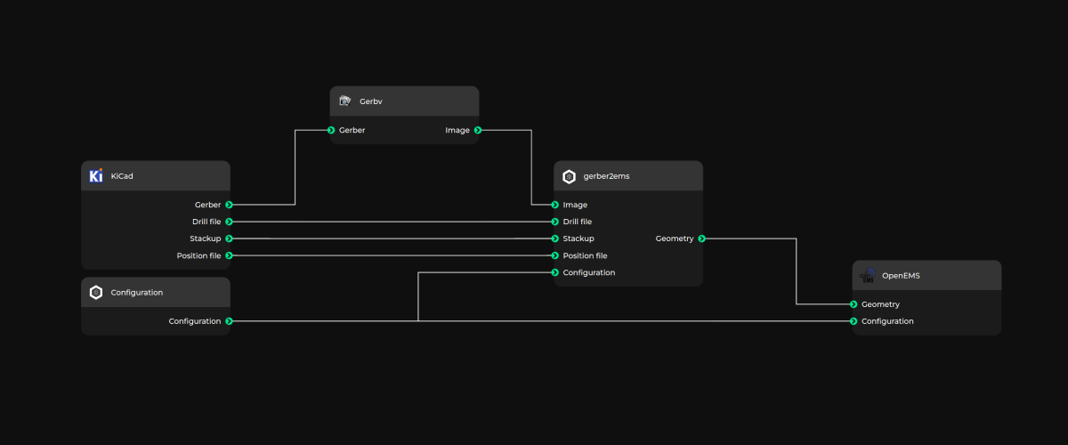
Antmicro, however, has been working on a completely open and automated hardware design flow, and EMS is an important element that was missing. To close this gap, we developed a script called gerber2ems that translates PCB fabrication files (generated for example by KiCad), an open source hardware design suite, into a three-dimensional mesh which can be processed with openEMS.
Below, we will review the basic principles of signal integrity analysis with OpenEMS, provide an overview of how the script works and the process of using our open source hardware test board to validate simulation output. We also show an example visualizations that workflow enables.
Simulating high-speed PCB traces with open source software
OpenEMS simulates the propagation of electromagnetic waves in a three-dimensional space defined by a mesh. Individual primitives of the mesh are assigned conductive or dielectric material properties. This geometry is derived from a PCB’s Gerber file, with adjustments made to represent passive components such as capacitors. In order to evaluate signal propagation in a trace, excitation and termination ports need to be defined. These additional, virtual PCB elements are derived from a schematic and components’ pad positions, and passed to the simulation preparation script via config files.
OpenEMS simulates propagation of electromagnetic waves resulting from the source port excitation, using the FDTD method, a discrete, time-domain based approach to solving Maxwell equations. The outcome can be then transformed to scattering parameters or trace impedance in the frequency domain.
Electromagnetic field simulation provides engineers with design-specific data which can be used for validation and optimization of high-frequency PCB designs in a much tighter feedback loop. This simulation-based approach can minimize the number of re-spins needed, reducing costs and development time. And as we are happy to see, given proper integration, OpenEMS provides a fully functional and open source alternative to proprietary electromagnetic simulation software.
Processing the simulation data
To even get started with using open source EMS in your hardware development flow, you need to represent your board in a way that OpenEMS can understand. The PCB fabrication files need to be processed by the newly developed gerber2ems script and later simulated to extract useful parameters from the design, such as S-parameters, impedance etc. They can then be automatically visualized with charts or plots which provide hardware teams with a comprehensive overview of the properties of the high-speed circuitry.

What is interesting, very compelling visualizations of the obtained output can be produced by importing it into the open source Blender 3D creation suite in order to create a detailed and easy to analyze three dimensional animated representation of the simulation, as shown below.
Using simulation provides a set of values describing the accuracy of a designed circuit in terms of signal integrity. The circuit can be then improved before it is manufactured. The automation of the process ensures a consistent hardware test environment in which the design can go through as many iterations as required. This iterative flow minimizes the probability of signal integrity issues during initial board testing and enhances the confidence in the correctness of the design, reducing the need for prototype re-spins and considerably saving overall project time.
For detailed instructions on using the gerber2ems script and processing the results, refer to the project’s README.
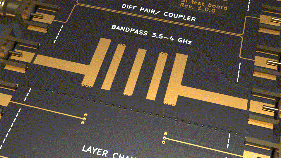
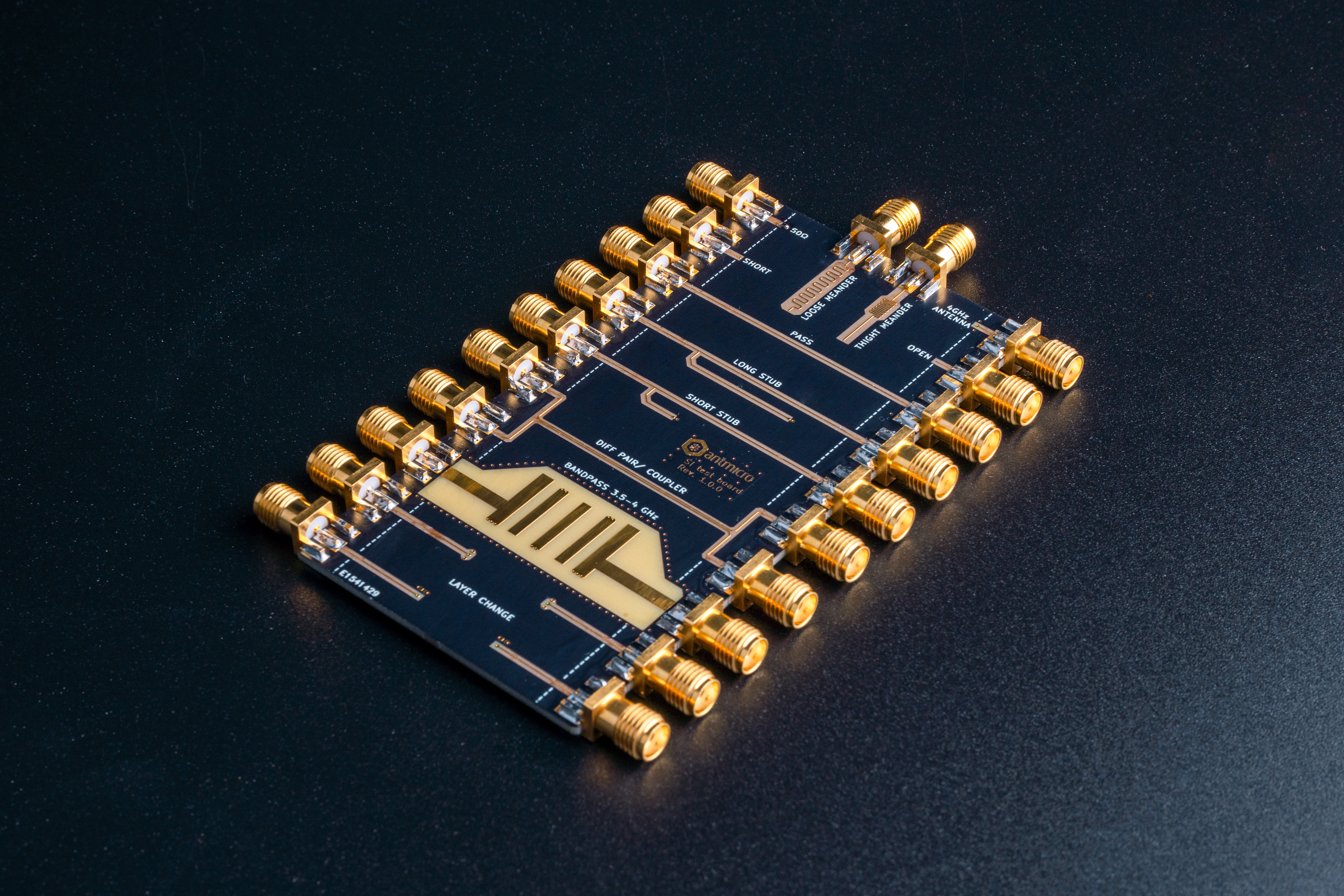
Verification with a reference SI test board
Antmicro developed a reference board as a sample device under test for the EMS solution. The board consists of isolated high-frequency trace test cases which we were able to individually analyze and simulate. It also allowed us to verify the simulation results with measurement of the physical object.
The reference board is available both on our Open Hardware Portal and on GitHub, meaning that users can use it to verify validity of the results on their own, focusing on parameters that are the most important for them.
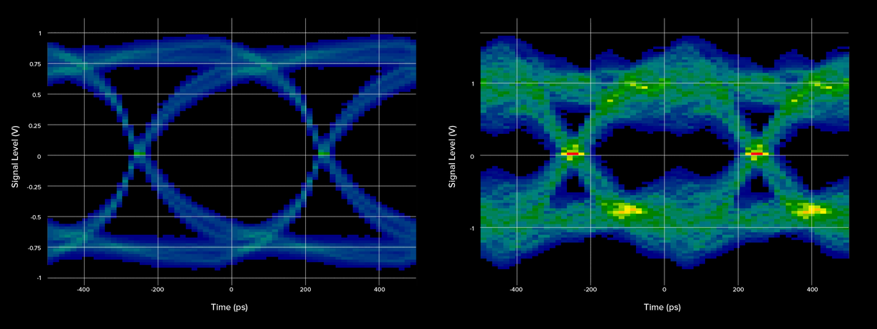
Eye diagrams
One of the most useful tools in an SI engineer’s arsenal is what’s called an eye diagram, which helps assess data link performance at a glance. It is constructed by superimposing time-domain voltage traces onto each other, with a trigger set on the signal edges. This way, all possible signal transitions are visualized. A wider “eye” means that it will be easier for the receiver to recover the clock and correctly sample the data. With a more open “eye”, the data link is less susceptible to noise. In the extreme case, the eye is completely closed and no data can be recovered.
Using the gerber2ems script output together with PyBert we can calculate what the signal’s eye diagram would look like after passing through the channel. Below you can see a comparison of eye diagrams of straight-through (left) and short stub (right) traces from our test board.
Closing the design loop with open source tooling and automation
By adding OpenEMS into our hardware design process with the help of our gerber2ems tool, we can close the loop of the end-to-end open source flow that we use to build advanced PCBs. This will enable collaborative access to the capability of detecting potential issues in a high-speed design process, which has huge implications for a more CI, software-driven flow. The EMS simulation helps develop more complex designs which, in our case, include DDR4 and DDR5 memories, high speed FPGAs and SoCs, quicker and more reliably.
Subsequent improvements to the project will focus on increasing the amount of automation available through creation of scripts allowing for automatic port placement and applying the correct terminations as necessary. There will also be further optimization relating to mesh generation as we move from uniform mesh to non-uniform mesh, adapted locally according to the position of the simulated traces, in order to increase the performance of the tools. This work will enable the provision of a SI simulation flow for the designs on our Open Hardware Portal, which will provide users with simulation data for a wide range of hardware.
Shortening the hardware development process means that we can assist our clients in bringing new products to market quicker as well as improving design consistency by automating flows within new or existing CI systems. We provide comprehensive PCB design services, while we also develop open source tools for specific use cases, as well as adapt and integrate existing tools for customer use in a similar manner as in the case of openEMS.
If you want to take advantage of Antmicro’s engineering services for building complex devices reliably and transparently, reach out to us at contact@antmicro.com.